
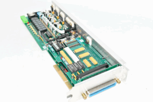
The process of cloning or duplicating an industrial robot controller card involves several technically challenging steps:
-
Multilayer Reconstruction
Most controller PCBs are multilayered, with internal signal and power layers that are not visible to the naked eye. Recovering the Gerber file, schematic diagram, and layout drawing often requires destructive techniques like layer-by-layer sanding or X-ray scanning to capture the internal routing and structure. -
Component Identification and BOM Recovery
Many ICs and passive components may have proprietary markings or be obsolete. Accurately generating the BOM list is difficult without a functioning reference or documentation. Reverse engineering must also account for exact footprint and electrical characteristics. -
Netlist and CAD File Generation
Once the schematic is reconstructed, a netlist must be verified against the cloned PCB design to ensure signal accuracy. Creating accurate CAD files requires expertise in PCB design software and attention to layout tolerances. -
Firmware and Logic Control
Controller cards often contain embedded firmware that cannot be accessed or copied directly due to read protection or encryption. This makes reproducing the full functionality difficult unless a working image or emulated firmware is available.
बहुपरत पुनर्निर्माण अधिकांश नियंत्रक PCB बहुपरत होते हैं, जिनमें आंतरिक सिग्नल और पावर परतें होती हैं जो नग्न आंखों को दिखाई नहीं देती हैं। गेरबर फ़ाइल, योजनाबद्ध आरेख और लेआउट ड्राइंग को पुनर्प्राप्त करने के लिए अक्सर आंतरिक रूटिंग और संरचना को कैप्चर करने के लिए परत-दर-परत सैंडिंग या एक्स-रे स्कैनिंग जैसी विनाशकारी तकनीकों की आवश्यकता होती है। घटक पहचान और BOM पुनर्प्राप्ति कई IC और निष्क्रिय घटकों में मालिकाना चिह्न हो सकते हैं या वे अप्रचलित हो सकते हैं। कार्यशील संदर्भ या दस्तावेज़ीकरण के बिना BOM सूची को सटीक रूप से बनाना मुश्किल है। रिवर्स इंजीनियरिंग को सटीक पदचिह्न और विद्युत विशेषताओं को भी ध्यान में रखना चाहिए। नेटलिस्ट और CAD फ़ाइल जनरेशन एक बार योजनाबद्ध पुनर्निर्माण हो जाने के बाद, सिग्नल सटीकता सुनिश्चित करने के लिए क्लोन किए गए PCB डिज़ाइन के विरुद्ध नेटलिस्ट को सत्यापित किया जाना चाहिए। सटीक CAD फ़ाइलें बनाने के लिए PCB डिज़ाइन सॉफ़्टवेयर में विशेषज्ञता और लेआउट सहनशीलता पर ध्यान देने की आवश्यकता होती है।
Below Figure summarizes the approach previously described for Grounding Mixed-Signal Devices with Low DC in Multilayer PCB Card Cloning. The analog ground plane is not corrupted because the small digital transient currents flow in the small loop between VD, the decoupling capacitor, and DGND (shown as a heavy line).
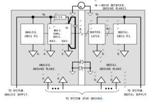
Grounding Mixed Signal ICs with Low Internal Digital Currents Multilayer PCB Card Cloning
The mixed signal device is for all intents and purposes treated as an analog component. The noise VN between the ground planes
reduces the noise margin at the digital interface but is generally not harmful if kept less than 300 mV by using a low impedance digital ground plane all the way back to the system star ground.
However, mixed-signal devices such as sigma-delta ADCs, codecs, and DSPs with on-chip analog functions are becoming more and more digitally intensive. Along with the additional digital circuitry come larger digital currents and noise. For example, a sigma- delta ADC or DAC contains a complex digital filter which adds considerably to the digital current in the device.
다층 재구성 대부분의 컨트롤러 PCB는 다층 구조로 되어 있으며, 육안으로는 볼 수 없는 내부 신호 및 전원 층이 있습니다. 거버 파일, 회로도, 레이아웃 도면을 복구하려면 내부 배선 및 구조를 파악하기 위해 층별 샌딩이나 X선 스캐닝과 같은 파괴적인 기법이 필요한 경우가 많습니다. 부품 식별 및 BOM 복구 많은 IC 및 수동 부품에는 독점 표시가 있거나 폐기된 부품이 있을 수 있습니다. 작동하는 참조 자료나 문서 없이는 BOM 목록을 정확하게 생성하는 것이 어렵습니다. 역엔지니어링은 정확한 풋프린트 및 전기적 특성도 고려해야 합니다. 넷리스트 및 CAD 파일 생성 회로도를 재구성한 후에는 신호 정확성을 보장하기 위해 복제된 PCB 설계와 넷리스트를 비교 검증해야 합니다. 정확한 CAD 파일을 생성하려면 PCB 설계 소프트웨어에 대한 전문 지식과 레이아웃 허용 오차에 대한 주의가 필요합니다. 펌웨어 및 로직 제어 컨트롤러 카드에는 읽기 보호 또는 암호화로 인해 직접 액세스하거나 복사할 수 없는 내장 펌웨어가 포함되어 있는 경우가 많습니다. 따라서 작동하는 이미지나 에뮬레이션된 펌웨어가 없으면 전체 기능을 재현하기 어렵습니다.
The method previously discussed depends on the decoupling capacitor between VD and DGND to keep the digital transient currents and isolated in a small loop. However, if the digital currents are significant enough and have components at dc or low frequencies, the decoupling capacitor may have to be so large that it is impractical. Any digital current which flows outside the loop between VD and DGND must flow through the analog ground plane. This may degrade performance, especially in high resolution systems.
It is difficult to predict what level of digital current flowing into the analog ground plane will become unacceptable in a system. All we can do at this point is to suggest an alternative grounding method which may yield better performance.
Even after successfully cloning the design, remanufacturing the PCB presents its own challenges:
-
Precision fabrication is required for fine traces, BGA components, and high-layer-count stack-ups
-
Controlled impedance and EMI mitigation must be maintained during the board layout and fabrication
-
Functional testing must simulate real robotic motion to validate the performance and timing of the control signals
-
Environmental durability, including temperature and vibration tolerance, must match industrial standards
Moreover, when reverse engineering a robot controller card, even minor deviations in trace width, component placement, or grounding strategy can lead to communication errors, motion instability, or hardware failures in the robotic system.
Industrial robot controller card cloning is far more than simply copying a PCB—it requires deep insight into embedded systems, real-time control, and multilayer PCB architecture. While the process can be time-consuming and technically demanding, it remains a crucial option for maintaining critical automation systems, especially when replacement parts are no longer available or supported. With precision, the cloned card can restore or even enhance the functionality of robotic systems that would otherwise face costly downtime or obsolescence.
La mayoría de las PCB de controlador son multicapa, con capas internas de señal y potencia invisibles a simple vista. Recuperar el archivo Gerber, el diagrama esquemático y el plano de diseño a menudo requiere técnicas destructivas como el lijado capa por capa o el escaneo por rayos X para capturar el enrutamiento y la estructura internos. Identificación de Componentes y Recuperación de la Lista de Materiales (BOM) Muchos circuitos integrados (CI) y componentes pasivos pueden tener marcas propietarias o estar obsoletos. Generar la lista de materiales con precisión es difícil sin una referencia o documentación funcional. La ingeniería inversa también debe considerar la huella exacta y las características eléctricas. Generación de Lista de Redes y Archivos CAD Una vez reconstruido el esquema, se debe verificar la lista de redes con el diseño de la PCB clonada para garantizar la precisión de la señal. Crear archivos CAD precisos requiere experiencia en software de diseño de PCB y prestar atención a las tolerancias de diseño.


