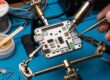

When a surround-view or front camera module goes end-of-life, the vehicle platform that depends on it does not. The practical path back to a working spare is to map ADAS camera circuit board hardware from a single physical sample: recover the copper geometry, trace every net, rebuild the BOM and schematic, then prove the copy performs like the original. This guide walks hardware engineers and purchasers through that process for automotive camera modules — the small, coax-fed boards built around an image sensor, a serializer, and a tightly regulated power section.
What Makes an ADAS Camera Board Different from a Consumer Module
An ADAS camera is not a webcam with a tougher housing. Its electrical character is dictated by three constraints that rarely appear together on a consumer board: it runs off a single coaxial cable that carries both power and a multi-gigabit video stream, it sits in an unconditioned automotive environment, and every signal that leaves the board travels over a long, noisy harness into an ECU. Each of those constraints shapes the reverse-engineering work.
Start with power. The module is fed through Power-over-Coax (PoC): a 4–17 V DC supply and a 3–6 Gbps GMSL or FPD-Link III serial stream share one 50 Ω FAKRA coax. On the board, a PoC filter — typically a bias inductor in series with the center conductor plus a bank of bypass capacitors — separates the DC supply path from the AC video path. Miss the inductor value or its saturation current and the clone will brown out when the serializer draws its peak current. Behind that filter, a tiny PMIC (often a TPS62xxx-class buck) and two or three low-noise LDOs generate the 3.3 V, 1.8 V, 1.3 V and 2.9 V rails the serializer and image sensor demand. The 2.9 V analog rail for the sensor is particularly unforgiving: ripple there shows up directly as fixed-pattern noise in the image.
Signal integrity is the second constraint. The image sensor outputs four MIPI CSI-2 lanes (D-PHY at roughly 1.5–2.5 Gbps per lane, or C-PHY) that run only a few centimeters to the serializer. The serializer then launches a single differential pair at 3 Gbps (GMSL1), 6 Gbps (GMSL2) or beyond toward the ECU. Those pairs are impedance-controlled to 100 Ω differential and 50 Ω single-ended, and they are routed away from the PoC bias tee and the switching PMIC to control return loss. For background on handling pairs like these, our note on differential signal handling techniques covers the layout rules that matter most.
EMC and the environment close the list. A 6 Gbps SerDes is a potent broadband radiator, and the board must meet CISPR 25 Class 5 radiated limits inside a vehicle. That means a shielded FAKRA interface, common-mode chokes on the coax, Pi-filtering on every rail, and symmetric routing so the differential pair does not become a monopole. Everything is built to AEC-Q100 Grade 1 (−40 °C to +105 °C) and often potted or conformally coated. Our write-up on PCB EMC design for reverse-engineered boards explains how those filters are reconstructed. The safety angle — link-loss detection, CRC, ASIL-rated diagnostics — lives mostly in firmware, which we do not copy; the hardware clone is pursued as compliant reverse engineering for legacy automotive hardware.
Teardown, Imaging, and Layer Reconstruction
Most ADAS camera modules are 6 to 12 layers with blind and buried vias, and the active devices — image sensor and serializer — are BGAs or CSPs with pads only visible under the package. The first job is to remove any conformal coating. Acrylic coatings lift in isopropanol in 15–30 minutes; silicone and parylene need mechanical peeling or a gel stripper. Once bare, the board is optically scanned at 2400 DPI per outer layer.
Inner layers are revealed by progressive delayering on a sacrificial sample, photographed at each step and stitched into a dimensionally accurate CAD image. Because automotive boards carry impedance-controlled pairs, micro-sectioning at several via locations is mandatory: it confirms dielectric thickness, copper weight (often 0.5–1 oz on signal layers, heavier on the PoC feed), and the exact stack-up. X-ray is used throughout to locate buried vias, confirm BGA pad connections under the sensor, and read the value marking on the PoC bias inductor when it is screened out by the coating. For the multilayer workflow itself, see our page on reverse engineering multilayer PCB boards.
How to Map ADAS Camera Circuit Board Nets and Identify Devices
With the geometry captured, the next step is connectivity. A flying-probe or continuity tester builds the netlist pad-by-pad, and the engineer groups nets into functional blocks. The hardest traces are the CSI-2 lanes escaping from under the BGA image sensor to the serializer, and the serializer’s single output pair running to the FAKRA connector — both are dense, impedance-controlled, and easy to misread if a buried via is missed.
Device identification is where these boards surprise people. The serializer (a MAX96717- or DS90UB953-class part) and the PMIC are usually marked, but the LDOs, the PoC bias inductor, the clock crystal, and any discrete protection can be screened or unmarked. We characterize them with LCR measurement, X-ray, and — only when necessary and with client consent — decapsulation. The I2C/CCI configuration bus that the ECU uses to program the sensor must be traced too, because its pull-ups and level shifters define how the clone initializes. Critically, the engineer must separate the DC PoC path from the AC video path at the coax entry; confusing the two is the single most common reason a first-pass clone fails to link.
Rebuilding the BOM and Schematic
Every component is identified by manufacturer part number, package, and value, then compiled into a BOM with AEC-Q100-qualified alternates and lifecycle flags (active, NRND, obsolete). Where a part is discontinued, the engineer selects a drop-in or near-drop-in replacement and notes the deviation explicitly — never silently.
The schematic is rebuilt by functional block: the PoC front-end (bias tee, bypass, TVS), the PMIC and LDO tree, the image sensor with its decoupling and clock, the serializer with its reference and configuration straps, and the FAKRA interface with its impedance-controlled pairs. Connector pinouts are annotated to match the vehicle harness side, which is what lets the recovered board drop back into the original loom. The method we use for this step is described in our guide to restoring a schematic from a physical PCB.
Prototype Fabrication and Functional Verification
Recovered Gerbers go to fabrication at the appropriate IPC class — most camera modules are Class 2, but safety-relevant modules may need Class 3 tolerances — and the assembled prototype is tested against the original sample. Verification is not “does it power on.” We measure every rail under load, confirm the PoC voltage reaches the serializer, check the MIPI CSI-2 lanes for a clean eye, confirm the SerDes achieves and holds lock, and capture a live image at both ambient and temperature extremes. Only when the clone matches the original across that checklist do we release the engineering package. The full loop — from Gerbers to a validated board — is covered on our prototype production and functional verification page.
Common Pitfalls in ADAS Camera Board Cloning
These boards fail in predictable ways, and most failures trace to a handful of mistakes:
- PoC filter mis-extracted. The bias inductor’s value or saturation current is read wrong, so the clone’s supply sags when the serializer transmits at peak power.
- Impedance wrong on the SerDes pair. A missed dielectric layer or wrong copper weight collapses the eye diagram and the link never locks.
- Missing BGA via or pad. One dropped CSI-2 lane means a dark or torn image even when everything else is correct.
- Wrong LDO output. Swapping the 1.8 V and 2.9 V rails, or using a noisy buck where a low-noise LDO belongs, leaves the sensor unable to initialize or adds visible noise.
- Conformal-coating residue. Incomplete removal hides silkscreen and traps moisture, causing intermittent shorts after assembly.
- FAKRA pinout assumed. The coax center/ground and any diagnostics pins vary by module; guessing them breaks PoC or the back-channel.
Frequently Asked Questions
How long does it take to map an ADAS camera board?
Timeline depends on layer count, coating, and whether the sample is unique. A typical 6–8 layer module runs a few weeks from intake to a validated prototype; 10–12 layer boards with buried vias take longer because micro-sectioning and delayering need more passes.
Can you clone the image sensor exactly?
The image sensor is almost always a standard Sony or OmniVision automotive part, which we source directly rather than copy. We do not extract or reproduce firmware; the clone replicates the board and bill of materials so a known-good sensor drops in.
Do you need the deserializer or ECU side too?
Not strictly. The camera board can be recovered from the module alone. Having the deserializer side helps us verify the SerDes link during validation, but it is optional and we can work from the camera sample and its datasheets.
What about firmware and functional safety (ASIL)?
Our scope is the hardware: Gerbers, BOM, and schematic. Where the original carries read-protected firmware or ASIL-rated diagnostics, those are handled by the customer’s own software and safety process. We pursue this work as compliant reverse engineering and repair support for legacy and obsolete hardware.
Is reverse engineering an ADAS camera board legal?
When the goal is to keep legacy or end-of-life hardware serviceable — for repair support, sparing, or redesign — and it is done without circumventing protections on third-party IP beyond what the law allows, it is a standard, compliant engineering service. We assess each project on that basis before intake.
If you are supporting a vehicle program that has lost its camera-module source, the fastest route to a verified spare is a disciplined effort to map ADAS camera circuit board hardware from a sample you already own. Our team recovers Gerbers, BOM, and schematic, then validates the clone against the original across temperature and load. Visit our automotive PCB reverse engineering services to discuss your module, or contact us to request a quotation and arrange to send a sample.