Cloning printed circuit board layout design provides critical value when original design data such as schematic diagrams, Gerber files, or CAD files are unavailable or no longer supported by the original manufacturer. In many industries—such as industrial automation, elevators, power systems, medical equipment, and transportation—electronic products remain operational for many years beyond the design lifecycle of their PCB boards. By reverse engineering and cloning the PCB layout, engineers can accurately recover the physical and electrical structure of the electronic circuit board, enabling continued manufacturing, maintenance, and system reliability without dependence on obsolete suppliers.

Klonowanie projektu płytki drukowanej ma kluczowe znaczenie, gdy oryginalne dane projektowe, takie jak schematy, pliki Gerber lub CAD, są niedostępne lub nie są już obsługiwane przez pierwotnego producenta. W wielu branżach – takich jak automatyka przemysłowa, windy, systemy energetyczne, sprzęt medyczny i transport – produkty elektroniczne pozostają sprawne przez wiele lat po zakończeniu cyklu życia ich płytek PCB. Dzięki inżynierii wstecznej i klonowaniu układu PCB inżynierowie mogą dokładnie odtworzyć fizyczną i elektryczną strukturę płytki drukowanej, co umożliwia ciągłą produkcję, konserwację i niezawodność systemu bez uzależnienia od przestarzałych dostawców. Klonowanie projektu płytki PCB stwarza również możliwości udoskonalenia projektu i optymalizacji wydajności. Po odzyskaniu oryginalnego układu płytki drukowanej inżynierowie mogą analizować integralność sygnału, dystrybucję mocy, właściwości termiczne i kompatybilność elektromagnetyczną. Na podstawie tej analizy sklonowaną płytkę PCB można zmodyfikować, ulepszyć lub zregenerować z wykorzystaniem nowoczesnych komponentów i ulepszonych materiałów. Proces ten przekształca kopiowanie PCB z prostej duplikacji w usługę inżynierską o wartości dodanej, umożliwiając zwiększoną niezawodność, wydłużony okres eksploatacji i dostosowanie do nowych wymagań technicznych przy jednoczesnym zachowaniu oryginalnej logiki systemu.
Another major value of PCB layout cloning lies in ensuring operational continuity and reducing downtime. When a key PCB board fails and no replacement is available, production lines, infrastructure systems, or mission-critical equipment may be forced to stop. Through precise PCB reverse engineering, engineers can extract netlists, recreate layout drawings, and generate new Gerber data to duplicate or reproduce the original PCB board. This capability allows companies to restore functionality quickly, minimize economic loss, and maintain stable operation, especially in environments where equipment availability directly impacts safety or productivity.

A clonagem do layout de placas de circuito impresso (PCBs) oferece um valor crucial quando os dados originais do projeto, como diagramas esquemáticos, arquivos Gerber ou arquivos CAD, não estão disponíveis ou não são mais suportados pelo fabricante original. Em muitos setores — como automação industrial, elevadores, sistemas de energia, equipamentos médicos e transporte — os produtos eletrônicos permanecem operacionais por muitos anos além do ciclo de vida do projeto de suas PCBs. Ao realizar a engenharia reversa e clonar o layout da PCB, os engenheiros podem recuperar com precisão a estrutura física e elétrica da placa de circuito eletrônico, permitindo a continuidade da fabricação, manutenção e confiabilidade do sistema sem depender de fornecedores obsoletos. A clonagem do layout da PCB também cria oportunidades para aprimoramento do projeto e otimização do desempenho. Uma vez recuperado o layout original da placa de circuito impresso, os engenheiros podem analisar a integridade do sinal, a distribuição de energia, o comportamento térmico e a compatibilidade eletromagnética. Com base nessa análise, a PCB clonada pode ser modificada, atualizada ou remanufaturada usando componentes modernos e materiais aprimorados. Esse processo transforma a cópia de PCBs de uma simples duplicação em um serviço de engenharia de valor agregado, possibilitando maior confiabilidade, vida útil prolongada e adaptação a novos requisitos técnicos, preservando a lógica original do sistema.
Cloning Printed Circuit Board Layout design has its long-term economic interests behind such a prevalence in the industry. In the process of PCB Board development, the cost of PCB Layout design accounts for more than one-half of the total Research and development cost. In the reverse research of existing products, the cost will be greatly reduced, and the corresponding research and development cycle will be significantly shortened, thus bringing huge economic benefits to the enterprise. The cost and market price of other electronic consumer products that naturally depend on PCB Board will also be reduced accordingly, which will continue to stimulate the domestic electronic consumer market.

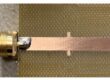
PCB Board layout design is an important part of pcb product development. In industrial applications, it generally refers to the layout and routing of electronic components on the PCB board layout after determining the schematic diagram of the pcb circuit board, and the ideal layout is designed to achieve the desired performance. The factors to be considered include the size of the printed circuit board and components, the interface, the number of wiring layers and the line width, and electromagnetic compatibility. In the process, designers often need to spend a long time and energy.

인쇄회로기판(PCB) 레이아웃 설계 복제는 회로도, 거버 파일, CAD 파일과 같은 원본 설계 데이터를 구할 수 없거나 제조사에서 더 이상 지원하지 않을 때 매우 중요한 가치를 제공합니다. 산업 자동화, 엘리베이터, 전력 시스템, 의료 장비, 운송 등 많은 산업 분야에서 전자 제품은 PCB 기판의 설계 수명 주기보다 훨씬 오랫동안 사용됩니다. PCB 레이아웃을 역설계하고 복제함으로써 엔지니어는 전자 회로기판의 물리적 및 전기적 구조를 정확하게 복원할 수 있으며, 이를 통해 더 이상 사용되지 않는 공급업체에 의존하지 않고 지속적인 제조, 유지보수 및 시스템 신뢰성을 확보할 수 있습니다. PCB 레이아웃 설계 복제는 또한 설계 개선 및 성능 최적화의 기회를 창출합니다. 원본 PCB 레이아웃을 복원한 후에는 신호 무결성, 전력 분배, 열 거동 및 전자기 호환성을 분석할 수 있습니다. 이러한 분석을 바탕으로 복제된 PCB는 최신 부품과 개선된 재료를 사용하여 수정, 업그레이드 또는 재제조할 수 있습니다. 이러한 과정을 통해 PCB 복제는 단순한 복제를 넘어 부가가치 엔지니어링 서비스로 전환되어, 원래 시스템 로직을 유지하면서 신뢰성 향상, 서비스 수명 연장, 새로운 기술 요구 사항에 대한 적응성을 가능하게 합니다.
Secondly is Overcome technical barriers and break market monopolies
PCB Board design companies often encounter such technical bottlenecks in the product development process, and those key technologies are often in the hands of enterprises in the industry, so it is easy to form a market monopoly. Reverse Engineering PCB Board Layout Design on the market can quickly eliminate technical bottlenecks, and update or upgrade on the basis of the original technology, so as to launch their own new products and effectively maintain the competitive situation in the market.

Клонирование компоновки печатной платы имеет решающее значение, когда исходные проектные данные, такие как принципиальные схемы, файлы Gerber или файлы САПР, недоступны или больше не поддерживаются производителем. Во многих отраслях — таких как промышленная автоматизация, лифты, энергетические системы, медицинское оборудование и транспорт — электронные изделия остаются работоспособными в течение многих лет после истечения срока службы их печатных плат. Путем обратного проектирования и клонирования компоновки печатной платы инженеры могут точно восстановить физическую и электрическую структуру электронной платы, что позволяет продолжать производство, техническое обслуживание и обеспечивать надежность системы без зависимости от устаревших поставщиков. Клонирование компоновки печатной платы также создает возможности для улучшения конструкции и оптимизации производительности. После восстановления исходной компоновки печатной платы инженеры могут проанализировать целостность сигналов, распределение питания, тепловые характеристики и электромагнитную совместимость. На основе этого анализа клонированная печатная плата может быть модифицирована, модернизирована или переизготовлена с использованием современных компонентов и улучшенных материалов. Этот процесс превращает копирование печатных плат из простого дублирования в ценную инженерную услугу, обеспечивающую повышенную надежность, увеличенный срок службы и адаптацию к новым техническим требованиям при сохранении исходной логики системы.
Cloning PCB layout design also creates opportunities for design improvement and performance optimization. Once the original printed circuit board layout is recovered, engineers can analyze signal integrity, power distribution, thermal behavior, and electromagnetic compatibility. Based on this analysis, the cloned PCB can be modified, upgraded, or remanufactured using modern components and improved materials. This process transforms PCB copying from simple duplication into a value-added engineering service, enabling enhanced reliability, extended service life, and adaptation to new technical requirements while preserving the original system logic.

Việc sao chép thiết kế bố cục mạch in (PCB) mang lại giá trị quan trọng khi dữ liệu thiết kế gốc như sơ đồ mạch, tệp Gerber hoặc tệp CAD không có sẵn hoặc không còn được nhà sản xuất gốc hỗ trợ. Trong nhiều ngành công nghiệp—như tự động hóa công nghiệp, thang máy, hệ thống điện, thiết bị y tế và vận tải—các sản phẩm điện tử vẫn hoạt động trong nhiều năm sau vòng đời thiết kế của bo mạch PCB. Bằng cách phân tích ngược và sao chép bố cục PCB, các kỹ sư có thể khôi phục chính xác cấu trúc vật lý và điện của bo mạch điện tử, cho phép tiếp tục sản xuất, bảo trì và độ tin cậy của hệ thống mà không phụ thuộc vào các nhà cung cấp lỗi thời. Việc sao chép thiết kế bố cục PCB cũng tạo ra cơ hội để cải tiến thiết kế và tối ưu hóa hiệu suất. Sau khi khôi phục được bố cục mạch in gốc, các kỹ sư có thể phân tích tính toàn vẹn tín hiệu, phân phối điện năng, hành vi nhiệt và khả năng tương thích điện từ. Dựa trên phân tích này, PCB được sao chép có thể được sửa đổi, nâng cấp hoặc sản xuất lại bằng cách sử dụng các linh kiện hiện đại và vật liệu được cải tiến. Quá trình này biến việc sao chép PCB từ việc sao chép đơn giản thành một dịch vụ kỹ thuật giá trị gia tăng, cho phép tăng cường độ tin cậy, kéo dài tuổi thọ và thích ứng với các yêu cầu kỹ thuật mới trong khi vẫn bảo toàn logic hệ thống ban đầu.
From a strategic and economic perspective, PCB layout cloning helps organizations protect investments and reduce long-term costs. Replacing entire electronic systems is often far more expensive than reproducing a specific PCB board. By cloning and reproducing printed circuit boards, companies can avoid costly redesign cycles, extend the usable life of legacy equipment, and maintain supply chain independence. When conducted responsibly and in compliance with intellectual property regulations, PCB layout cloning becomes a practical and ethical solution that supports sustainable manufacturing, technical continuity, and long-term asset management.

La clonación del diseño de la placa de circuito impreso (PCB) aporta un valor crucial cuando los datos de diseño originales, como diagramas esquemáticos, archivos Gerber o archivos CAD, no están disponibles o el fabricante original ya no los ofrece. En muchos sectores, como la automatización industrial, los ascensores, los sistemas de energía, los equipos médicos y el transporte, los productos electrónicos permanecen operativos durante muchos años, incluso después del ciclo de vida útil de sus placas PCB. Mediante ingeniería inversa y clonación del diseño de la PCB, los ingenieros pueden recuperar con precisión la estructura física y eléctrica de la placa de circuito electrónico, lo que permite la fabricación, el mantenimiento y la fiabilidad del sistema sin depender de proveedores obsoletos. La clonación del diseño de la PCB también ofrece oportunidades para la mejora del diseño y la optimización del rendimiento. Una vez recuperado el diseño original de la placa de circuito impreso, los ingenieros pueden analizar la integridad de la señal, la distribución de la energía, el comportamiento térmico y la compatibilidad electromagnética. Con base en este análisis, la PCB clonada puede modificarse, actualizarse o remanufacturarse con componentes modernos y materiales mejorados. Este proceso transforma la copia de PCB, de una simple duplicación, en un servicio de ingeniería de valor añadido, que permite una mayor fiabilidad, una mayor vida útil y la adaptación a nuevos requisitos técnicos, preservando al mismo tiempo la lógica original del sistema.