
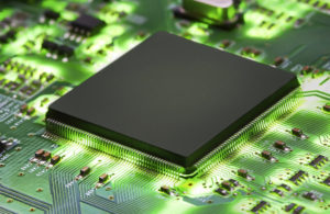
Designing high-density printed circuit boards (HDI PCBs) is critical for modern electronics, especially in advanced fields like military defense. These boards pack intricate circuitry into minimal space, enabling compact, high-performance systems. However, achieving this requires overcoming challenges such as signal integrity, thermal management, and component placement. This article explores key strategies for HDI PCB design, focusing on applications like graphic modules for military defense, and highlights how reverse engineering techniques play a role in refining these complex systems.
Das Design hochdichter Leiterplatten (HDI-Leiterplatten) ist für moderne Elektronik, insbesondere in anspruchsvollen Bereichen wie der militärischen Verteidigung, von entscheidender Bedeutung. Diese Leiterplatten vereinen komplexe Schaltungen auf kleinstem Raum und ermöglichen so kompakte, leistungsstarke Systeme. Um dies zu erreichen, müssen jedoch Herausforderungen wie Signalintegrität, Wärmemanagement und Bauteilplatzierung bewältigt werden. Dieser Artikel untersucht wichtige Strategien für das Design von HDI-Leiterplatten mit Schwerpunkt auf Anwendungen wie Grafikmodulen für die militärische Verteidigung und zeigt, wie Reverse-Engineering-Techniken zur Verfeinerung dieser komplexen Systeme beitragen.
Challenges in High-Density PCB Design
1. Miniaturization Without Compromise
HDI PCBs demand ultra-thin traces, microvias, and stacked layers to accommodate components like BGAs (Ball Grid Arrays) and fine-pitch ICs. Designers must balance:
Signal integrity – Preventing crosstalk and EMI through careful trace spacing and shielding.
Thermal dissipation – Integrating thermal vias and heatsinks to manage heat in densely packed layouts.
Manufacturability – Ensuring designs align with fabrication capabilities to avoid defects.
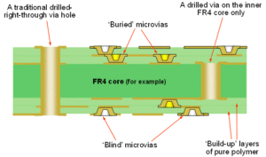
2. Layer Stacking and Material Selection
Military-grade HDI PCBs often use specialized materials like polyimide or ceramic substrates for high-temperature stability. Multilayer stackups (10+ layers) are common to isolate analog, digital, and power sections, reducing interference.
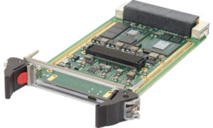
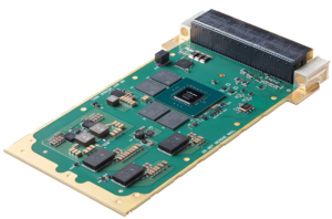
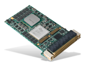
Graphic Modules for Military Defense: A Case Study
Military systems rely on HDI PCBs for graphic modules that process real-time data in applications like:
Surveillance drones – High-resolution imaging and video processing.
Targeting systems – Rapid rendering of 3D terrain maps.
Communication hubs – Secure data transmission with low latency.
Bu tür modülleri tasarlamak, donanım-yazılım entegrasyonunu optimize etmek için ürün yazılımı mühendisleriyle iş birliği yapmayı gerektirir. HDI PCB Geliştirmede Tersine Mühendislik Teknikleri Eski askeri sistemlerde dokümantasyon eksikliği olduğunda, tersine mühendislik teknikleri paha biçilmez hale gelir. Örneğin: Tarama ve Görüntüleme – Dahili izleri ve geçiş yollarını haritalamak için X-ışını veya 3B tarama kullanma. Bileşen Analizi – Veri sayfası çapraz referanslama yoluyla IC’leri ve pasif parçaları belirleme. Sinyal Araştırması – Devre işlevselliğini yeniden oluşturmak için osiloskoplarla dalga formlarını analiz etme. Tersine mühendislik yalnızca eski sistemleri onarmaya yardımcı olmakla kalmaz, aynı zamanda FPGA hızlandırıcıları gibi modern bileşenlerle grafik modüllerinin yükseltilmesi için de içgörüler sağlar. Termal ve Mekanik Hususlar Savunma sistemlerindeki HDI PCB’ler aşırı koşullarla karşı karşıyadır. Tasarımcılar şunları yapmalıdır: Termal profilleri simüle edin – ANSYS gibi araçlar sıcak noktaları tahmin eder ve soğutucu yerleşimini optimize eder. Konformal kaplamalar kullanın – Nem, toz ve kimyasal maruziyete karşı koruyun. Sert-esnek tasarımlar uygulayın – Havacılık sistemlerinde kompakt, dayanıklı düzenler için sert ve esnek PCB’leri birleştirin.
These modules require:
High-speed interfaces – PCIe, LVDS, or HDMI for fast data transfer.
Radiation-hardened components – To withstand harsh environments.
EMI shielding – Preventing signal degradation in mission-critical operations.
Designing such modules involves collaboration with firmware engineers to optimize hardware-software integration.
Reverse Engineering Techniques in HDI PCB Development
When legacy military systems lack documentation, reverse engineering techniques become invaluable. For example:
Scanning and Imaging – Using X-ray or 3D scanning to map internal traces and vias.
Component Analysis – Identifying ICs and passive parts through datasheet cross-referencing.
Signal Probing – Analyzing waveforms with oscilloscopes to reconstruct circuit functionality.
Reverse engineering not only aids in repairing obsolete systems but also provides insights for upgrading graphic modules with modern components like FPGA accelerators.
Thermal and Mechanical Considerations
HDI PCBs in defense systems face extreme conditions. Designers must:
Simulate thermal profiles – Tools like ANSYS predict hotspots and optimize heatsink placement.
Use conformal coatings – Protect against moisture, dust, and chemical exposure.
Implement rigid-flex designs – Combine rigid and flexible PCBs for compact, durable layouts in aerospace systems.
La conception de circuits imprimés haute densité est essentielle au développement des technologies de défense militaire, notamment pour les modules graphiques nécessitant un traitement ultra-compact et rapide. En combinant un empilement de couches innovant, des matériaux avancés et des techniques de rétro-ingénierie, les ingénieurs peuvent surmonter les obstacles de conception et fournir des solutions fiables pour les applications critiques. À mesure que les systèmes militaires évoluent, les circuits imprimés HDI resteront à la pointe, permettant une électronique plus intelligente, plus compacte et plus résiliente. En maîtrisant ces principes, les concepteurs peuvent garantir que leurs circuits imprimés HDI répondent aux exigences rigoureuses des systèmes de défense modernes tout en ouvrant la voie aux innovations de nouvelle génération.
Design for Manufacturing (DFM) Best Practices
To avoid costly delays:
Collaborate with fabricators early – Confirm trace/space tolerances and via sizes.
Test prototypes rigorously – Validate signal performance under simulated military conditions.
Leverage automation – Auto-routing tools for complex layouts, paired with manual adjustments.
High density PCB Board designing is increasingly challenged by several factors: physical, finer pitch pin spacing, in-surfficient financial support, mounting must be very precise, and the environment limitation.
Many plastic packages absorb moisture, causing the crack on assembly processing. Physical factors also include the complexity of the installation process and the reliability of the final product. Further financial decisions must consider how the PCB board will be manufactured and assembled.
More fragile pin components, such as SQFP, shrink quad flat packs with 0.50 and 0.40mm?0.020” and 0.016” pin pitches, may be it will present a challenge to an assembly specialist in maintaining consistent assembly process qualification rate.
High Density PCB board designing
The most successful development plans are the high density PCB board design guidelines and pad geometries that have already undergone process certification.
In terms of environment, the pad geometries may be different and it is based on the type of welding used to mount the electronic parts. When it becomes possible, the pad shape should be defined in a way that is transparent to the mounting process used.
Whether the parts are mounted on one or both sides of the PCB board, subjected to wave soldering, reflow soldering, or other methods, the pad and part dimensions should be optimized to ensure proper solder joints and inspection criteria.
high density circuit board design
Although the soldering patterns are dimensionally defined, and because it is part of geometry shape of printed circuit board, they are limited by the level of producibility and the tolerances associated with plating, corrosion, assembly, or other conditions.
The productivity aspect is also related to the use of the solder mask and the alignment of the solder mask to the conductor pattern.


