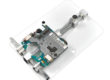
Restoring a printed circuit board (PCB) without a schematic diagram can be a challenging task, especially when dealing with complex electronics. However, with the right techniques and tools, it is possible to diagnose faults, repair damaged traces, and bring a non-functional PCB back to life. This guide provides practical steps to restore printed circuit board without schematic diagram effectively.

Restaurar uma placa de circuito impresso (PCB) sem um diagrama esquemático pode ser uma tarefa desafiadora, especialmente quando se trata de componentes eletrônicos complexos. No entanto, com as técnicas e ferramentas corretas, é possível diagnosticar falhas, reparar trilhas danificadas e trazer uma PCB com defeito de volta à vida. Este guia fornece etapas práticas para restaurar uma placa de circuito impresso sem diagrama esquemático de forma eficaz.
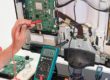
1. Visual Inspection
The first step in PCB restoration is a thorough visual inspection. Look for obvious signs of damage, such as:
-
Burnt or discolored components
-
Broken or lifted traces
-
Corroded or oxidized solder joints
-
Swollen or leaking capacitors
Using a magnifying glass or microscope can help identify tiny cracks or solder bridges that may cause malfunctions.
2. Clean the PCB
Dirt, dust, and corrosion can interfere with conductivity. Clean the PCB using:
-
Isopropyl alcohol (90% or higher) and a soft brush
-
Deionized water for stubborn residues
-
Compressed air to remove debris from tight spaces
Ensure the board is completely dry before proceeding.
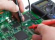
3. Check for Short Circuits and Open Traces
Without a schematic, you’ll need to manually trace connections:
-
Use a multimeter in continuity mode to check for open or shorted traces.
-
Compare with a known-working PCB (if available) to identify discrepancies.
-
Follow copper pathways to understand component interconnections.
4. Test and Replace Faulty Components
-
Diodes & Transistors: Check forward and reverse bias using a multimeter.
-
Resistors & Capacitors: Measure values and replace if out of tolerance.
-
ICs & Microcontrollers: Test voltage at pins or swap with a known-good chip if possible.
Desolder damaged components carefully and replace them with matching specifications.

Baskılı devre kartını (PCB) şematik diyagram olmadan onarmak, özellikle karmaşık elektroniklerle uğraşırken zorlu bir görev olabilir. Ancak doğru teknikler ve araçlarla arızaları teşhis etmek, hasarlı izleri onarmak ve çalışmayan bir PCB’yi hayata döndürmek mümkündür. Bu kılavuz, baskılı devre kartını şematik diyagram olmadan etkili bir şekilde onarmak için pratik adımlar sağlar.
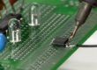
5. Repair Damaged Traces
If a trace is broken:
-
Scrape off solder mask to expose copper.
-
Use thin wire or conductive pen to bridge the gap.
-
Secure with solder and cover with insulating varnish.
6. Power Up and Test Gradually
Before full power-up:
-
Use a current-limited power supply to avoid further damage.
-
Check for overheating components.
-
Measure voltages at key test points.
If the PCB still fails, revisit previous steps for missed faults.

Odnawianie płytki drukowanej (PCB) bez schematu może być trudnym zadaniem, szczególnie w przypadku skomplikowanej elektroniki. Jednak przy użyciu odpowiednich technik i narzędzi możliwe jest zdiagnozowanie usterek, naprawa uszkodzonych ścieżek i przywrócenie niedziałającej płytki PCB do życia. Ten przewodnik zawiera praktyczne kroki skutecznego przywracania płytki drukowanej bez schematu.
Conclusion
Restoring a PCB without a schematic diagram requires patience, methodical testing, and attention to detail. By following these steps—visual inspection, cleaning, continuity checks, component testing, trace repair, and gradual power testing—you can successfully restore printed circuit board without schematic diagram and extend the lifespan of electronic devices.
When try to Restore Printed Circuit Board in the absence of its schematic diagram, especially when this Printed Circuit Board is relatively strange to the engineer, according to previous experience, even if a veteran Printed Circuit Board restoring engineer won’t be able to fix this issue promptly and smoothly, hereby we list some of the main principles that can be followed when try to repair a one to increase the working efficiency:
First of all, monitor target Printed Circuit Board and then measure it, the tools should be applied include the multi-meter and microscopy, the good habit to handling a Printed circuit board ready to be restored is monitoring it, by using microscopy can check if there is any break-off of tracks on the Printed Circuit Board;

Restore Printed Circuit Board without Schematic Diagram
And if there is any break-off phenomenons can be found on the negative parts such as resistor, electros, transistor, diode and triode; and the most important thing is if this Printed circuit board had been restored before.
If yes then which components had been touched or moved? Is there any mis-conduct such as false soldering, cold soldering or reverse insertion, after confirming there is no such case, need to use multi-meter to test the resistance value among the power supply and ground, normally this value of resistance could be around 70 to 80 ohm, or above,

cuando se intenta restaurar la placa de circuito impreso en ausencia de su diagrama esquemático, especialmente cuando esta placa de circuito impreso es relativamente extraña para el ingeniero, según la experiencia previa, incluso si un ingeniero veterano de restauración de placas de circuito impreso no podrá solucionar este problema de manera rápida y sin problemas, a continuación enumeramos algunos de los principios fundamentales que se pueden seguir cuando se intenta reparar una para aumentar la eficiencia de trabajo:
if the resistance value is too small, only a handful or a dozen of ohm, there could be some of the components have been breakdown,
then it is necessary to find out the breakdown components from the Printed circuit boards, and the method is power on it, and feel the temperature of each one of them, and those with extremely high temperature will become suspected item.
And if the resistance value is normal, need to measure the value of each part such as resistor, diode, triode and MOS-field effect tube, switch. The purpose is to ensure the