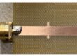
The process of designing and manufacturing communication interface PCB boards for industrial conveyor systems requires extreme precision, particularly when it comes to PCB Board Drilling. Each hole in a printed circuit board (PCB) plays a critical role—whether it is used for mounting components, forming vias, or connecting multi-layer copper traces. For engineers engaged in reverse engineering, cloning, or remanufacturing these boards, understanding proper drilling design rules ensures both electrical performance and mechanical reliability in the final prototype.

इलेक्ट्रॉनिक सर्किट बोर्ड के उत्पादन में, ड्रिलिंग यह निर्धारित करती है कि विभिन्न घटक और परतें किस प्रकार परस्पर क्रिया करती हैं। एक संचार इंटरफ़ेस बोर्ड में आमतौर पर सिग्नल कनेक्टर, ट्रांसीवर और आइसोलेशन सर्किट शामिल होते हैं जिनके लिए सटीक छेद प्लेसमेंट और प्लेटिंग की आवश्यकता होती है। यदि इंजीनियर ऐसे डिज़ाइन की प्रतिकृति बनाने या उसे पुनर्स्थापित करने का प्रयास करते हैं, तो लेआउट ड्राइंग या गेरबर फ़ाइल में त्रुटियाँ मिसअलाइनमेंट, खराब सोल्डरिंग या खुले सर्किट का कारण बन सकती हैं। इसलिए, इंजीनियर पुनरुत्पादन से पहले प्रत्येक ड्रिल छेद के स्थान, आकार और सहनशीलता को सत्यापित करने के लिए नेटलिस्ट, कैड फ़ाइल और गेरबर डेटा का सावधानीपूर्वक विश्लेषण करते हैं। किसी मौजूदा पीसीबी की रिवर्स इंजीनियरिंग करते समय, इंजीनियर अक्सर ऑप्टिकल या एक्स-रे उपकरणों का उपयोग करके छेदों के आकार को मापते और दर्ज करते हैं। डिज़ाइन को संशोधित करते समय या पुनर्प्राप्ति या दोहराव के लिए एक नई गेरबर फ़ाइल बनाते समय यह डेटा महत्वपूर्ण होता है। जब इंजीनियर किसी मौजूदा संचार इंटरफ़ेस पीसीबी बोर्ड की रिवर्स इंजीनियरिंग करते हैं, तो एक बड़ी चुनौती सटीक ड्रिल परत स्टैक-अप और वाया गहराई का पता लगाने में होती है। ब्लाइंड और दबे हुए वाया अक्सर आंतरिक परतों के बीच छिपे रहते हैं, जिससे मूल गेरबर डेटा के संदर्भ के बिना उसी छेद संरचना का पुनरुत्पादन करना मुश्किल हो जाता है। सटीक ड्रिलिंग डेटा को पुनर्स्थापित करने के लिए कभी-कभी उन्नत इमेजिंग टूल या माइक्रोसेक्शनिंग तकनीकों की आवश्यकता होती है। क्लोन बोर्ड को अलग-अलग घटकों या कनेक्टर्स के साथ संशोधित करते समय एक और चुनौती उत्पन्न होती है। किसी भी नए छेद को विद्युत निकासी और सिग्नल अखंडता को बनाए रखते हुए विनिर्माण मानकों का पालन करना होगा। यदि सावधानीपूर्वक विश्लेषण नहीं किया गया तो पुनर्निर्माण के दौरान किए गए समायोजन यांत्रिक माउंटिंग या ईएमआई परिरक्षण को प्रभावित कर सकते हैं।
Importance of Drilling in PCB Design
In electronic circuit board production, drilling defines how different components and layers interact. A communication interface board typically includes signal connectors, transceivers, and isolation circuits that require accurate hole placement and plating. If engineers attempt to replicate or restore such a design, errors in the layout drawing or Gerber file can cause misalignment, poor soldering, or open circuits. Therefore, engineers carefully analyze the netlist, cad file, and Gerber data to verify the location, size, and tolerance of each drill hole before reproduction.
When reverse engineering an existing PCB, engineers often measure and document hole sizes using optical or X-ray equipment. This data is crucial when modifying the design or generating a new Gerber file for recovery or duplication.
In below articles we would like to introduce some of the PCB Board drilling tips which can help designer not only decrease the production cost but increase the reliability of PCB Board:
The inner diameter of the through hole is required to be 0.2mm (8mil) or more in principle, and the outer diameter is 0.4mm (16mil) or more. In difficult places, it must be controlled to an outer diameter of 0.35mm (14mil);
Tip small assistant: According to the experience, the inner diameter and outer diameter of the commonly used via size of PCB generally follow X*2±2mil (X indicates the inner diameter). For example, a 8 mil inner diameter via can be designed as 8/14 mil, 8/16 mil or 8/18 mil; for example, a 12 mil via can be designed as 12/22 mil, 12/24 mil, 12/26 mil;

Trong sản xuất bảng mạch điện tử, quá trình khoan xác định cách các thành phần và lớp khác nhau tương tác với nhau. Một bảng mạch giao tiếp thường bao gồm các đầu nối tín hiệu, bộ thu phát và mạch cách ly, đòi hỏi vị trí lỗ khoan và lớp mạ chính xác. Nếu các kỹ sư cố gắng sao chép hoặc khôi phục thiết kế như vậy, các lỗi trong bản vẽ bố trí hoặc tệp Gerber có thể gây ra sai lệch, hàn kém hoặc hở mạch. Do đó, các kỹ sư cần phân tích cẩn thận danh sách mạng, tệp CAD và dữ liệu Gerber để xác minh vị trí, kích thước và dung sai của từng lỗ khoan trước khi tái tạo. Khi thiết kế ngược một PCB hiện có, các kỹ sư thường đo và ghi lại kích thước lỗ khoan bằng thiết bị quang học hoặc X-quang. Dữ liệu này rất quan trọng khi sửa đổi thiết kế hoặc tạo tệp Gerber mới để phục hồi hoặc sao chép. Khi các kỹ sư thiết kế ngược một bảng mạch PCB giao tiếp hiện có, một thách thức lớn nằm ở việc phát hiện chính xác độ sâu của lớp khoan và độ dày của lỗ khoan. Các lỗ khoan mù và lỗ khoan chôn thường ẩn giữa các lớp bên trong, khiến việc tái tạo cùng một cấu trúc lỗ mà không tham chiếu đến dữ liệu Gerber gốc trở nên khó khăn. Đôi khi cần đến các công cụ hình ảnh tiên tiến hoặc kỹ thuật vi phẫu để khôi phục dữ liệu khoan chính xác. Một thách thức khác phát sinh khi sửa đổi bo mạch sao chép để bao gồm các thành phần hoặc đầu nối khác nhau. Bất kỳ vị trí lỗ mới nào cũng phải tuân thủ các tiêu chuẩn sản xuất, đồng thời vẫn đảm bảo khoảng hở điện và tính toàn vẹn của tín hiệu. Các điều chỉnh được thực hiện trong quá trình tái sản xuất có thể ảnh hưởng đến việc lắp ráp cơ học hoặc khả năng che chắn EMI nếu không được phân tích kỹ lưỡng.
When reverse engineering PCB with BGA footprint recommendations in 0.65mm and above, do not use buried or blind holes, the cost will increase significantly. When using a blind hole, a phase 1 blind hole is generally used (TOP layer – L2 layer or BOTTOM – negative L2). The inner diameter of the via hole is generally 0.1 mm (4 mil) and the outer diameter is 0.25 mm (10 mil). See below Figure.

The via hole cannot be placed on the pad of less than 0402 resistor capacity pad; theoretically, the lead inductance on the pad is small, but when it is produced, the solder paste is easy to enter the via hole, causing the solder paste to be uneven and causing the electronic component to assemble onto the PCB unevenly. Generally recommended spacing is 4-8mil.

Effective PCB Board Drilling starts with a strong understanding of hole function and manufacturing limits. The following design principles are commonly applied when engineers remanufacture or reproduce communication interface boards:
-
Drill Size Selection: Component leads must fit comfortably into plated holes. Oversized holes can weaken solder joints, while undersized ones cause assembly difficulties. For signal connectors, engineers typically reserve tight mechanical tolerances in the cad file.
-
Aspect Ratio Control: The ratio between the PCB thickness and hole diameter affects plating quality. A poor ratio may result in incomplete copper plating inside holes, compromising electrical continuity.
-
Via Hole Precision: In multilayer boards, via holes must align perfectly between internal layers to ensure correct netlist connectivity. Misalignment may cause shorts or signal loss in high-speed communication lines.
-
Drill-to-Copper Clearance: Engineers define minimum spacing between drill holes and copper features in the layout drawing to prevent electrical arcing or manufacturing defects.
-
Tool Wear and Tolerance: Drill bit wear affects hole accuracy. During prototype PCB production, regular tool calibration is necessary to maintain consistency.
Challenges in Reverse Engineering Drilled Holes
When engineers reverse engineer an existing communication interface PCB board, one major challenge lies in detecting the exact drill layer stack-up and via depth. Blind and buried vias often remain hidden between inner layers, making it difficult to reproduce the same hole structure without reference to the original Gerber data. Advanced imaging tools or microsectioning techniques are sometimes required to restore accurate drilling data.
Another challenge occurs when modifying a cloned board to include different components or connectors. Any new hole placement must comply with manufacturing standards while maintaining electrical clearance and signal integrity. Adjustments made during remanufacture can affect mechanical mounting or EMI shielding if not carefully analyzed.

전자 회로 기판 생산에서 드릴링은 다양한 부품과 레이어의 상호 작용 방식을 정의합니다. 통신 인터페이스 기판에는 일반적으로 정확한 홀 배치 및 도금이 필요한 신호 커넥터, 트랜시버, 절연 회로가 포함됩니다. 엔지니어가 이러한 설계를 복제하거나 복원하려고 할 경우, 레이아웃 도면이나 거버 파일의 오류로 인해 정렬 불량, 납땜 불량 또는 회로 단선이 발생할 수 있습니다. 따라서 엔지니어는 재현 전에 넷리스트, CAD 파일, 거버 데이터를 신중하게 분석하여 각 드릴 홀의 위치, 크기 및 공차를 확인합니다. 기존 PCB를 역설계할 때 엔지니어는 광학 장비나 X선 장비를 사용하여 홀 크기를 측정하고 기록하는 경우가 많습니다. 이 데이터는 설계를 수정하거나 복구 또는 복제를 위해 새로운 거버 파일을 생성할 때 매우 중요합니다. 엔지니어가 기존 통신 인터페이스 PCB 기판을 역설계할 때 가장 큰 과제 중 하나는 정확한 드릴 레이어 스택업과 비아 깊이를 감지하는 것입니다. 블라인드 비아와 매립 비아는 내부 레이어 사이에 숨겨져 있는 경우가 많아 원본 거버 데이터를 참조하지 않고 동일한 홀 구조를 재현하기 어렵습니다. 정확한 드릴링 데이터를 복원하려면 고급 이미징 도구나 미세 절편 기술이 필요한 경우가 있습니다. 복제된 보드에 다른 부품이나 커넥터를 포함하도록 수정할 때 또 다른 문제가 발생합니다. 새로운 구멍 배치는 전기적 간격과 신호 무결성을 유지하면서 제조 표준을 준수해야 합니다. 재제조 과정에서 조정된 내용은 신중하게 분석하지 않으면 기계적 장착이나 EMI 차폐에 영향을 미칠 수 있습니다.
Benefits of Accurate Drilling Design
Proper PCB Board Drilling ensures stable signal transmission, reliable soldering, and strong mechanical bonding of components on the printed circuit board. For conveyor systems that rely on consistent communication between sensors, controllers, and actuators, precision-drilled holes minimize vibration stress and prevent electrical disconnections. Furthermore, well-documented Gerber files, BOM lists, and schematic diagrams allow for seamless duplication, recovery, and long-term reproduction of spare boards.
Conclusion
Mastering PCB Board Drilling Tips is an essential skill for engineers working on communication interface PCB boards. Whether the project involves reverse engineering, cloning, or remanufacturing, attention to drilling accuracy determines the durability and performance of the final electronic circuit board. Through precise Gerber file preparation, careful layout drawing review, and strict adherence to mechanical tolerances, engineers can replicate and restore boards that perform as reliably as the original designs in demanding industrial conveyor applications.

電子回路基板の製造において、ドリル加工は異なる部品や層間の相互作用を決定づける要素です。通信インターフェース基板には通常、信号コネクタ、トランシーバー、絶縁回路などが搭載されており、正確な穴の配置とめっきが求められます。エンジニアがこのような設計を複製または復元しようとすると、レイアウト図やガーバーファイルのエラーにより、位置ずれ、はんだ付け不良、断線などが発生する可能性があります。そのため、エンジニアはネットリスト、CADファイル、ガーバーデータを慎重に分析し、複製前に各ドリル穴の位置、サイズ、許容誤差を検証します。既存のPCBをリバースエンジニアリングする際、エンジニアは光学機器やX線機器を用いて穴のサイズを測定し、記録することがよくあります。このデータは、設計を変更したり、復元や複製のために新しいガーバーファイルを生成したりする際に非常に重要です。エンジニアが既存の通信インターフェースPCB基板をリバースエンジニアリングする際の大きな課題の一つは、ドリル層の正確なスタックアップとビアの深さを検出することです。ブラインドビアやベリードビアは内層の間に隠れていることが多く、元のガーバーデータを参照せずに同じ穴構造を再現することは困難です。正確な掘削データを復元するには、高度な画像ツールや微細断面技術が必要となる場合があります。クローン基板に異なる部品やコネクタを追加するために改造する場合にも、新たな課題が生じます。新たな穴の配置は、電気的クリアランスと信号整合性を維持しながら、製造基準に準拠する必要があります。再製造中に行われた調整は、慎重に分析しないと、機械的な実装やEMIシールドに影響を与える可能性があります。