In the realm of electronics restoration, Reverse Engineering Circuit Board Material Analysis is a critical step when replicating or remanufacturing a PCB board without access to original design documents. This process goes beyond copying the Gerber file, layout drawing, or schematic diagram—it involves identifying and characterizing the base materials used in the printed circuit board (PCB) itself. Whether your goal is to clone, replicate, reproduce, or modify an existing electronic circuit board, understanding the underlying raw material and substrate composition is key to achieving functional and mechanical equivalence.

En nuestros servicios de ingeniería inversa, utilizamos una combinación de métodos de pruebas destructivos y no destructivos para analizar la estructura de PCB. Las técnicas clave incluyen:
Microscopía de sección transversal
Determina la superposición de capas, el espesor del cobre y la estructura de las vías
Ayuda a identificar si la PCB es HDI de una, dos o varias capas
Espectroscopía infrarroja por transformada de Fourier (FTIR)
Identifica el tipo de resina (p. ej., FR4, poliimida, PTFE, CEM-1, Rogers)
Útil para reproducir el comportamiento dieléctrico exacto en placas de alta frecuencia
Análisis termogravimétrico (TGA) y calorimetría diferencial de barrido (DSC)
Determina la temperatura de transición vítrea (Tg) y el punto de descomposición térmica
Garantiza que la placa clonada pueda soportar la misma carga térmica
Fluorescencia de rayos X (XRF)
Analiza la composición metálica de la superficie (cobre, estaño, oro, níquel, etc.)
Útil para definir el tipo de recubrimiento y el acabado superficial
Tomografía computarizada e inspección por rayos X
Mapea las capas internas sin dañar el prototipo
Apoya la reconstrucción de la lista de conexiones archivo cad y datos gerber
The material analysis, including chemical and metallurgical analysis, should be performed to determine the composition, surface treatments, finishes, hardness, and heat treatments pertinent to each piece-part/component. since circuit board can be made by various material from Fiber resin with glass cloth, the fiber resin can be classfied from rank 1 to rank 4, as well as inflamable level, dielectrical parameter, coefficient parameter, hardness, etc.
When working with industrial, aerospace, medical, or automotive PCB systems, different performance demands require different types of base materials. These materials determine:
-
Thermal conductivity
-
Dielectric constant
-
Signal integrity and EMI shielding
-
Mechanical strength and flexibility
-
Environmental resistance (humidity, temperature, vibration)
By conducting material analysis, we can ensure that a remanufactured or modified circuit board performs identically to the original—even under extreme conditions.
In our reverse engineering services, we use a combination of destructive and non-destructive testing methods to analyze the PCB structure. Key techniques include:
-

W naszych usługach inżynierii odwrotnej wykorzystujemy kombinację metod badań niszczących i nieniszczących w celu analizy struktury PCB. Kluczowe techniki obejmują:
Mikroskopia przekroju poprzecznego
Określa ułożenie warstw, grubość miedzi i strukturę przelotek
Pomaga zidentyfikować, czy płytka PCB jest jednostronna, dwustronna czy wielowarstwowa HDI
Spektroskopia w podczerwieni z transformacją Fouriera (FTIR)
Identyfikuje rodzaj żywicy (np. FR4, poliimid, PTFE, CEM-1, Rogers)
Przydatne w odtwarzaniu dokładnego zachowania dielektrycznego w płytkach o wysokiej częstotliwości
Analiza termograwimetryczna (TGA) i różnicowa kalorymetria skaningowa (DSC)
Określa temperaturę zeszklenia (Tg) i punkt rozkładu termicznego
Zapewnia, że sklonowana płytka wytrzyma takie samo obciążenie cieplne
Fluorescencja rentgenowska (XRF)
Analizuje skład powierzchniowego metalu (miedź, cyna, złoto, nikiel itp.)
Przydatne w określaniu rodzaju powłoki i wykończenia powierzchni
Skanowanie CT i kontrola rentgenowska
Mapuje wewnętrzne warstwy bez uszkadzania prototyp
Obsługuje rekonstrukcję listy połączeń, pliku CAD i danych GerberCross-Section Microscopy
-
Determines layer stack-up, copper thickness, and via structure
-
Helps identify if the PCB is single, double-sided, or multilayer HDI
-
-
Fourier Transform Infrared Spectroscopy (FTIR)
-
Identifies the type of resin (e.g., FR4, polyimide, PTFE, CEM-1, Rogers)
-
Useful in reproducing exact dielectric behavior in high-frequency boards
-
-
Thermogravimetric Analysis (TGA) and Differential Scanning Calorimetry (DSC)
-
Determines glass transition temperature (Tg) and thermal decomposition point
-
Ensures the cloned board can handle the same heat load
-
-
X-Ray Fluorescence (XRF)
-
Analyzes surface metal composition (copper, tin, gold, nickel, etc.)
-
Useful for defining the plating type and surface finish
-
-
CT Scanning & X-ray Inspection
-
Maps inner layers without damaging the prototype
-
Supports the reconstruction of netlist, cad file, and gerber data
-
Different circuit board raw material will be applied on various environment, for example, the high TG point material will normally used on the harsh and complicate scenario which need the electronic device to surface high temperature, high moisture, high salty level. regarding the other signal transmission scenario such as the antenna, signal relay basement, and signal amplifier, mobile signal station, teflon or ceramic material will be chosen for these kinds of scenarios, so before we reverse engineering circuit board received from customers, it is necessary to know its working environment and condition;

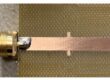
Reverse Engineering Circuit Board Material Analysis
Sample size
Reverse engineering PCB material presents several technical challenges:
-
Layer delamination: Older or heat-damaged PCBs may delaminate during analysis, making accurate measurement of substrate thickness difficult.
-
Proprietary materials: Some high-performance boards use custom laminates with undisclosed composition, requiring sophisticated identification tools.
-
Microvia inspection: HDI boards with blind/buried vias are difficult to assess without expensive 3D imaging.
-
Surface finish ambiguity: ENIG, HASL, OSP, or silver plating may appear visually similar but behave differently in reflow soldering and electrical performance.
Spectrographic samples should be submitted for composition analysis and identification of elements. The suggested sample size is: 1” X 1” X 1,” as smaller-sized samples are less cost efficient and may prohibit the use of instrumental analysis. The material analysis for plastic parts usually requires as much as one month additional time. Where possible, samples should be submitted in their entirety for metallurgical analysis. for some of the plastic or metal enclosure, if the internal structure is too small or complicate to be measured, engineer need to use the 3D scanning technique to get the 3D drawing of it for subsequent reverse engineering. Improper cutting of the sample could affect the hardness readings or the interpretation of the heat treating process.
After we complete Reverse Engineering Circuit Board Material Analysis, the data feeds directly into the remanufacturing phase. We recreate:
-

В наших услугах по обратному проектированию мы используем комбинацию методов разрушающего и неразрушающего тестирования для анализа структуры печатной платы. Ключевые методы включают:
Микроскопия поперечного сечения
Определяет расположение слоев, толщину меди и структуру переходных отверстий
Помогает определить, является ли печатная плата одно-, двухсторонней или многослойной HDI
Инфракрасная спектроскопия с преобразованием Фурье (FTIR)
Определяет тип смолы (например, FR4, полиимид, PTFE, CEM-1, Rogers)
Полезен для воспроизведения точного диэлектрического поведения в высокочастотных платах
Термогравиметрический анализ (TGA) и дифференциальная сканирующая калориметрия (DSC)
Определяет температуру стеклования (Tg) и точку термического разложения
Гарантирует, что клонированная плата может выдерживать ту же тепловую нагрузку
Рентгеновская флуоресценция (XRF)
Анализирует состав металла поверхности (медь, олово, золото, никель и т. д.)
Полезен для определения типа покрытия и отделки поверхности
КТ-сканирование и рентгеновский контроль
Картографирует внутренние слои, не повреждая прототип
Поддерживает реконструкцию списка соединений, файла CAD и данных GerberMultilayer PCB stack-up using identical materials
-
BOM list with matching dielectric and thermal characteristics
-
Gerber files that reflect correct trace width and copper weight
With this level of material accuracy, the replicated PCB meets all design and performance expectations—suitable for mission-critical applications.
Reverse engineering a circuit board isn’t just about tracing connections; it’s about understanding the soul of the board—its material. Whether you’re seeking to recover, restore, or remanufacture a legacy design, our expert PCB material analysis services deliver the reliability you need for seamless cloning and long-term performance.