PCB reverse engineering and IC reverse engineering are closely related disciplines within electronic system analysis, yet they operate at different technical layers. PCB reverse engineering focuses on the printed circuit board as a system-level carrier, analyzing how components are interconnected through copper traces, vias, and layers. By contrast, IC reverse engineering dives into the semiconductor itself, targeting the internal structure of an integrated circuit. In practice, these two approaches are often used together, especially when engineers need a complete understanding of a legacy electronic product or an unsupported industrial controller.

Ключевая связь между обратным проектированием печатных плат и обратным проектированием интегральных схем заключается в реконструкции системы. Обратное проектирование печатных плат позволяет инженерам восстанавливать принципиальные схемы, списки соединений, чертежи компоновки, файлы Gerber и спецификации материалов с существующей печатной платы. Это обеспечивает четкую карту потока сигналов, распределения питания и функциональных блоков на уровне платы. Однако, когда критически важная интегральная схема защищена, не документирована или снята с производства, одних данных с печатной платы может быть недостаточно. В таких случаях обратное проектирование интегральных схем дополняет процесс, выявляя микропрограммное обеспечение, логические структуры или внутренние конфигурации, которые напрямую влияют на работу печатной платы как полноценной электронной схемы. Несмотря на эту связь, техническая область применения и методология обратного проектирования печатных плат и обратного проектирования интегральных схем принципиально различны. Обратное проектирование печатных плат в значительной степени опирается на визуальный осмотр, электрическое тестирование и реконструкцию печатной платы в САПР. Оно в основном направлено на воспроизведение, дублирование или модификацию печатной платы для ремонта, разработки прототипов или восстановления. С другой стороны, обратное проектирование интегральных схем включает в себя передовые методы, такие как декапсуляция, анализ кристалла и извлечение встроенного ПО. Его цели часто включают в себя понимание внутренней логики, восстановление кода или обход механизмов безопасности, что выходит далеко за рамки физической компоновки печатной платы.
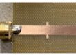
The reverse engineering essence is the process of obtaining technical information from the reverse analysis of products. There are mainly three kinds of reverse engineering in engineering technology practice, namely pcb reverse engineering, integrated circuit reverse engineering and reverse engineering of computer software. They maintain consistency in their thinking, but each has its own characteristics.

Here, the reason why they are listed together for comparison is to find the similarities and differences in their technical aspects, to fully explain the characteristics of pcb reverse engineering itself, and on the other hand to do some technical work in the field of legislative protection. After all, the law in the legislative is blank in terms of pcb layout design and circuit board reverse engineering, while integrated circuits and computer software have specific and relatively mature legislation on intellectual property protection. We can learn from these relatively mature legislative experiences. Providing conditions for intellectual property protection of PCB Layout drawing.

PCB 역설계와 IC 역설계의 핵심 연결 고리는 시스템 재구성이라는 점에 있습니다. PCB 역설계를 통해 엔지니어는 기존 PCB 기판에서 회로도, 넷리스트, 레이아웃 도면, 거버 파일, BOM 목록 등을 복구할 수 있습니다. 이를 통해 기판 수준에서 신호 흐름, 전력 분배, 기능 블록에 대한 명확한 지도를 얻을 수 있습니다. 그러나 중요한 IC가 보호되어 있거나, 관련 문서가 없거나, 단종된 경우에는 PCB 데이터만으로는 충분하지 않을 수 있습니다. 이러한 경우 IC 역설계는 펌웨어, 논리 구조, 내부 구성 등을 파악하여 PCB가 전체 전자 회로 기판으로서 어떻게 작동하는지에 직접적인 영향을 미치는 요소를 밝혀냄으로써 PCB 역설계를 보완합니다. 이러한 연결 고리에도 불구하고, PCB 역설계와 IC 역설계의 기술적 범위와 방법론은 근본적으로 다릅니다. PCB 역설계는 주로 육안 검사, 전기 테스트, CAD를 이용한 기판 재구성에 의존합니다. 주로 수리, 프로토타입 개발, 재제조를 위해 PCB를 복제, 모방 또는 수정하는 데 중점을 둡니다. 반면 IC 역설계는 디캡슐레이션, 다이 분석, 펌웨어 추출과 같은 고급 기술을 활용합니다. 이러한 공격의 목표는 종종 내부 논리를 이해하고, 코드를 복구하거나, 보안 메커니즘을 우회하는 것을 포함하며, 이는 단순히 PCB의 물리적 레이아웃을 파악하는 것 이상의 의미를 지닙니다.
The core connection between PCB reverse engineering and IC reverse engineering lies in system reconstruction. PCB reverse engineering enables engineers to recover schematic diagrams, netlists, layout drawings, Gerber files, and BOM lists from an existing PCB board. This provides a clear map of signal flow, power distribution, and functional blocks at the board level. However, when a critical IC is protected, undocumented, or discontinued, PCB data alone may be insufficient. In such cases, IC reverse engineering complements the process by revealing firmware, logic structures, or internal configurations that directly affect how the PCB operates as a complete electronic circuit board.

Kluczowym elementem łączącym inżynierię wsteczną PCB i inżynierię wsteczną układów scalonych jest rekonstrukcja systemu. Inżynieria wsteczna PCB umożliwia inżynierom odtworzenie schematów, list połączeń, rysunków układów, plików Gerber i list BOM z istniejącej płytki PCB. Zapewnia to przejrzysty obraz przepływu sygnału, dystrybucji zasilania i bloków funkcjonalnych na poziomie płytki. Jednakże, gdy krytyczny układ scalony jest zabezpieczony, nieudokumentowany lub wycofany z produkcji, same dane PCB mogą być niewystarczające. W takich przypadkach inżynieria wsteczna układów scalonych uzupełnia proces, ujawniając oprogramowanie układowe, struktury logiczne lub konfiguracje wewnętrzne, które bezpośrednio wpływają na działanie płytki PCB jako kompletnego układu elektronicznego. Pomimo tego związku, zakres techniczny i metodologia inżynierii wstecznej PCB i inżynierii wstecznej układów scalonych różnią się zasadniczo. Inżynieria wsteczna PCB opiera się w dużej mierze na inspekcji wizualnej, testach elektrycznych i rekonstrukcji CAD płytki drukowanej. Polega ona głównie na reprodukcji, duplikacji lub modyfikacji płytki PCB w celu naprawy, opracowania prototypu lub regeneracji. Inżynieria wsteczna układów scalonych z kolei obejmuje zaawansowane techniki, takie jak dekapsulacja, analiza matryc i ekstrakcja oprogramowania układowego. Jego celem jest często zrozumienie wewnętrznej logiki, odzyskanie kodu lub ominięcie mechanizmów bezpieczeństwa, które wykraczają daleko poza fizyczny układ płytki PCB.
Despite this connection, the technical scope and methodology of PCB reverse engineering and IC reverse engineering are fundamentally different. PCB reverse engineering relies heavily on visual inspection, electrical testing, and CAD reconstruction of the printed circuit board. It is mainly concerned with reproducing, duplicating, or modifying the PCB for repair, prototype development, or remanufacture. IC reverse engineering, on the other hand, involves advanced techniques such as decapsulation, die analysis, and firmware extraction. Its objectives often include understanding internal logic, recovering code, or bypassing security mechanisms, which go far beyond the physical layout of a PCB.

A principal conexão entre a engenharia reversa de PCBs e a engenharia reversa de CIs reside na reconstrução do sistema. A engenharia reversa de PCBs permite que os engenheiros recuperem diagramas esquemáticos, netlists, desenhos de layout, arquivos Gerber e listas de materiais (BOM) de uma placa de circuito impresso existente. Isso fornece um mapa claro do fluxo de sinal, distribuição de energia e blocos funcionais no nível da placa. No entanto, quando um CI crítico está protegido, não documentado ou descontinuado, os dados da PCB por si só podem ser insuficientes. Nesses casos, a engenharia reversa de CIs complementa o processo, revelando firmware, estruturas lógicas ou configurações internas que afetam diretamente o funcionamento da PCB como uma placa de circuito eletrônico completa. Apesar dessa conexão, o escopo técnico e a metodologia da engenharia reversa de PCBs e da engenharia reversa de CIs são fundamentalmente diferentes. A engenharia reversa de PCBs depende fortemente da inspeção visual, testes elétricos e reconstrução CAD da placa de circuito impresso. Ela se concentra principalmente em reproduzir, duplicar ou modificar a PCB para reparo, desenvolvimento de protótipos ou remanufatura. A engenharia reversa de CIs, por outro lado, envolve técnicas avançadas, como desencapsulamento, análise de chips e extração de firmware. Seus objetivos geralmente incluem a compreensão da lógica interna, a recuperação de código ou a burla de mecanismos de segurança, o que vai muito além do layout físico de uma placa de circuito impresso.
There are many differences in integrated circuit reverse engineering compare with PCB reverse engineering. Reverse engineering of integrated circuits, also known as reverse engineering of chips, refers to chip attackers relying on special equipment or self-made equipment to exploit loopholes or other defects in the design of integrated circuits. With the help of relevant professional technologies, the important files in the single-chip microprocessor are obtained such as the content inside the memory from flash and eeprom or other Key information such as security key or code, the ability to copy chip or disassemble the process yourself. IC reverse engineering involves three key technologies, namely sample pretreatment technology, chip analysis software technology and chip circuit analysis technology. These three technologies will directly affect the IC reverse engineering effect.

La conexión principal entre la ingeniería inversa de PCB y la ingeniería inversa de CI reside en la reconstrucción del sistema. La ingeniería inversa de PCB permite a los ingenieros recuperar diagramas esquemáticos, listas de conexiones, planos de diseño, archivos Gerber y listas de materiales de una placa PCB existente. Esto proporciona un mapa claro del flujo de señal, la distribución de potencia y los bloques funcionales a nivel de placa. Sin embargo, cuando un CI crítico está protegido, no está documentado o se descontinúa, los datos de la PCB por sí solos pueden ser insuficientes. En estos casos, la ingeniería inversa de CI complementa el proceso al revelar firmware, estructuras lógicas o configuraciones internas que afectan directamente el funcionamiento de la PCB como una placa de circuito electrónico completa. A pesar de esta conexión, el alcance técnico y la metodología de la ingeniería inversa de PCB y la ingeniería inversa de CI son fundamentalmente diferentes. La ingeniería inversa de PCB se basa en gran medida en la inspección visual, las pruebas eléctricas y la reconstrucción CAD de la placa de circuito impreso. Se centra principalmente en la reproducción, duplicación o modificación de la PCB para su reparación, desarrollo de prototipos o remanufactura. La ingeniería inversa de CI, por otro lado, implica técnicas avanzadas como la desencapsulación, el análisis de matrices y la extracción de firmware. Sus objetivos a menudo incluyen comprender la lógica interna, recuperar código o eludir mecanismos de seguridad, que van mucho más allá del diseño físico de una PCB.
In real-world projects, the distinction between these two disciplines determines project strategy and cost. PCB reverse engineering alone is often sufficient for clone or replicate tasks when standard components are used. However, when a system relies on custom or protected chips, IC reverse engineering becomes essential to achieve full recovery and functional reproduction. Together, PCB reverse engineering and IC reverse engineering form a complete technical pathway, allowing engineers to restore, reproduce, and modernize electronic systems with a high level of accuracy and reliability.

Mối liên hệ cốt lõi giữa kỹ thuật đảo ngược PCB và kỹ thuật đảo ngược IC nằm ở việc tái cấu trúc hệ thống. Kỹ thuật đảo ngược PCB cho phép các kỹ sư khôi phục sơ đồ mạch, danh sách mạng, bản vẽ bố trí, tệp Gerber và danh sách BOM từ một bo mạch PCB hiện có. Điều này cung cấp một bản đồ rõ ràng về luồng tín hiệu, phân phối nguồn và các khối chức năng ở cấp độ bo mạch. Tuy nhiên, khi một IC quan trọng được bảo vệ, không được ghi chép hoặc đã ngừng sản xuất, dữ liệu PCB đơn thuần có thể không đủ. Trong những trường hợp như vậy, kỹ thuật đảo ngược IC bổ sung cho quá trình này bằng cách tiết lộ phần mềm nhúng, cấu trúc logic hoặc cấu hình bên trong ảnh hưởng trực tiếp đến cách PCB hoạt động như một bo mạch điện tử hoàn chỉnh. Mặc dù có mối liên hệ này, phạm vi kỹ thuật và phương pháp luận của kỹ thuật đảo ngược PCB và kỹ thuật đảo ngược IC về cơ bản là khác nhau. Kỹ thuật đảo ngược PCB dựa nhiều vào kiểm tra trực quan, kiểm tra điện và tái tạo CAD của bo mạch in. Nó chủ yếu liên quan đến việc sao chép, nhân bản hoặc sửa đổi PCB để sửa chữa, phát triển nguyên mẫu hoặc tái sản xuất. Mặt khác, kỹ thuật đảo ngược IC liên quan đến các kỹ thuật tiên tiến như bóc vỏ, phân tích chip và trích xuất phần mềm nhúng. Mục tiêu của nó thường bao gồm việc hiểu logic bên trong, khôi phục mã hoặc vượt qua các cơ chế bảo mật, những điều này vượt xa bố cục vật lý của một bảng mạch in.