
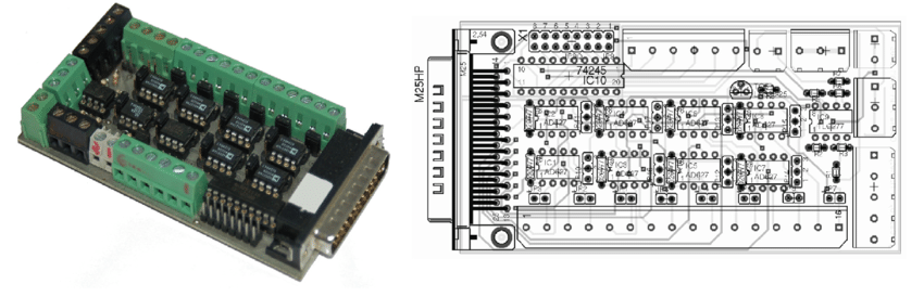
In the field of modern unmanned aerial systems (UAS), every function—from flight control to power distribution—relies on complex printed circuit boards (PCB). These boards integrate high-speed signal transmission, power management, and sensor communication within compact structures that must withstand vibration, electromagnetic interference, and extreme environmental conditions. To enhance system reliability and optimize performance, engineers often perform reverse engineering PCB techniques to analyze, restore, and reproduce existing UAV PCB layouts for improvement and modernization.

في مجال أنظمة الطائرات بدون طيار الحديثة (UAS)، تعتمد كل وظيفة – من التحكم في الطيران إلى توزيع الطاقة – على لوحات دوائر مطبوعة (PCB) معقدة. تدمج هذه اللوحات نقل الإشارات عالي السرعة، وإدارة الطاقة، واتصالات المستشعرات ضمن هياكل مدمجة تتحمل الاهتزازات والتداخل الكهرومغناطيسي والظروف البيئية القاسية. لتعزيز موثوقية النظام وتحسين الأداء، غالبًا ما يستخدم المهندسون تقنيات الهندسة العكسية للوحات الدوائر المطبوعة لتحليل واستعادة وإعادة إنتاج تصميمات لوحات الدوائر المطبوعة الحالية للطائرات بدون طيار لتحسينها وتحديثها. تبدأ عملية تحسين تصميم لوحات الدوائر المطبوعة لأنظمة الطائرات بدون طيار من خلال الهندسة العكسية بتحليل دقيق للوحة الدائرة الإلكترونية الأصلية. يفحص المهندسون المخطط التخطيطي، وملف Gerber، ورسم التصميم لفهم وضع المكونات، وتوجيه الإشارة، واستراتيجية توزيع الطاقة. في حال فقدان الوثائق الأصلية، مثل قائمة الشبكة، أو قائمة المواد، أو ملف CAD، يتم إعادة إنشاء ملفات التصميم هذه من خلال التحليل الفيزيائي والاختبار الكهربائي. تُمكّن عملية الاستعادة هذه المهندسين من تكرار أو نسخ النموذج الأولي للوحة الدوائر المطبوعة الحالية مع إدخال تحسينات في التصميم تُحسّن تبديد الحرارة، وتُقلل من اقتران الضوضاء، وتزيد من سلامة الإشارة.
The process to optimize unmanned aerial system PCB layout by reverse engineering PCB begins by carefully analyzing the original electronic circuit board. Engineers examine the schematic diagram, Gerber file, and layout drawing to understand component placement, signal routing, and power distribution strategy. When original documentation such as the netlist, BOM list, or CAD file is missing, these design files are recreated from physical analysis and electrical testing. This recovery process enables engineers to replicate or duplicate the existing prototype PCB board while introducing design optimizations that improve heat dissipation, reduce noise coupling, and increase signal integrity.
Many PCBs are no longer single-function circuits (digital or analog circuits), but rather a mixture of digital and analog circuits. Therefore, it is necessary to consider the mutual interference between them. through the obselete physical PCB sample, we can Optimize PCB Layout by Reverse Engineering PCB, obtain its original Gerber file and layout diagram. Especially the noise interference on the ground. The frequency of the digital circuit is high, and the sensitivity of the analog circuit is strong. For the signal line, the high-frequency signal line is as far as possible away from the sensitive analog circuit device.
For the ground line, the whole PCB layout drawing has only one node to the outside, so The problem of the number of processing and the common mode must be carried out inside the PCB, and the digital ground and the analog ground inside the board are actually separated from each other, but only at the interface where the PCB is connected to the outside (such as a plug). The digital ground is slightly shorted to the analog ground. Please note that there is only one connection point. There is also no common ground on the PCB, which is determined by the system design.

در حوزه سیستمهای هوایی بدون سرنشین مدرن (UAS)، هر عملکردی – از کنترل پرواز گرفته تا توزیع برق – به بردهای مدار چاپی (PCB) پیچیده متکی است. این بردها انتقال سیگنال پرسرعت، مدیریت برق و ارتباط حسگر را در ساختارهای فشردهای که باید در برابر لرزش، تداخل الکترومغناطیسی و شرایط محیطی شدید مقاومت کنند، ادغام میکنند. برای افزایش قابلیت اطمینان سیستم و بهینهسازی عملکرد، مهندسان اغلب تکنیکهای مهندسی معکوس PCB را برای تجزیه و تحلیل، بازیابی و بازتولید طرحهای PCB پهپاد موجود برای بهبود و نوسازی انجام میدهند. فرآیند بهینهسازی طرح PCB سیستم هوایی بدون سرنشین با مهندسی معکوس PCB با تجزیه و تحلیل دقیق برد مدار الکترونیکی اصلی آغاز میشود. مهندسان نمودار شماتیک، فایل Gerber و نقشه طرح را بررسی میکنند تا محل قرارگیری قطعات، مسیریابی سیگنال و استراتژی توزیع برق را درک کنند. هنگامی که اسناد اصلی مانند لیست شبکه، لیست BOM یا فایل CAD وجود ندارد، این فایلهای طراحی از تجزیه و تحلیل فیزیکی و آزمایش الکتریکی بازسازی میشوند. این فرآیند بازیابی به مهندسان این امکان را میدهد که برد PCB نمونه اولیه موجود را تکثیر یا کپی کنند و در عین حال بهینهسازیهای طراحی را معرفی کنند که اتلاف گرما را بهبود میبخشد، اتصال نویز را کاهش میدهد و یکپارچگی سیگنال را افزایش میدهد.
When wiring the multi-layer printed circuit board, there is not much space left in the signal line layer. If the number of layers is added, the waste will increase the workload and increase the cost. To resolve this contradiction, consider layout PCB board wiring on the electrical (ground) layer. The power layer should be considered first, followed by the ground layer. Because it is best to preserve the integrity of the formation.

In a large area of grounding (electricity), the pins of common components are connected to them, and the treatment of the connecting pins needs to be comprehensively considered. In terms of electrical performance, the pads of the component legs are perfectly connected with the copper surface, but There are some hidden dangers in the soldering assembly of the components. For example, 1st point is welding requires a high-power heater. 2nd is easy to cause a virtual solder joint. Therefore, taking into account the electrical performance and process needs, making a cross-shaped pad, called heat shield, commonly known as thermal pad, so that the possibility of creating a solder joint due to cross-distribution heat during soldering can be greatly reduced. The treatment of the grounding pin of the multi-layer PCB board is the same.
In high-speed UAV electronics, even the smallest layout modification can affect overall flight stability and data accuracy. Therefore, engineers apply strict reverse engineering principles to maintain the same electrical behavior while modifying trace geometry, grounding patterns, and via design to reduce electromagnetic interference. Through this remanufacture process, a redesigned PCB not only preserves the original system logic but also provides enhanced reliability and manufacturability.

У сфері сучасних безпілотних авіаційних систем (БПЛА) кожна функція — від керування польотом до розподілу живлення — залежить від складних друкованих плат (ДП). Ці плати інтегрують високошвидкісну передачу сигналів, керування живленням та зв’язок з датчиками в компактних структурах, які повинні витримувати вібрацію, електромагнітні перешкоди та екстремальні умови навколишнього середовища. Щоб підвищити надійність системи та оптимізувати продуктивність, інженери часто використовують методи зворотного проектування друкованих плат, щоб аналізувати, відновлювати та відтворювати існуючі схеми друкованих плат БПЛА для покращення та модернізації. Процес оптимізації схеми друкованих плат безпілотних авіаційних систем за допомогою зворотного проектування друкованих плат починається з ретельного аналізу оригінальної електронної плати. Інженери вивчають принципову схему, файл Gerber та креслення схеми, щоб зрозуміти розміщення компонентів, маршрутизацію сигналів та стратегію розподілу живлення. Коли оригінальна документація, така як список з’єднань, список специфікації або файл CAD, відсутня, ці файли проекту відтворюються на основі фізичного аналізу та електричних випробувань. Цей процес відновлення дозволяє інженерам відтворити або дублювати існуючий прототип друкованої плати, одночасно впроваджуючи оптимізації проекту, які покращують тепловіддачу, зменшують шумовий зв’язок та підвищують цілісність сигналу.
The optimization focuses on several key principles. First, engineers separate analog and digital domains in the PCB layout to minimize crosstalk and timing distortion. Second, power and ground planes are redesigned for more efficient current return paths, lowering the noise level on sensitive signals. Third, by reproducing the original schematic diagram and Gerber data, thermal management and impedance control can be improved without changing the functional architecture. The result is a new printed circuit board that meets or exceeds the performance of the original design while being easier to assemble and maintain.
During this reverse engineering PCB process, several challenges arise. Multi-layer UAV boards may contain buried or blind vias, making it difficult to extract an accurate layout drawing. High-density components and custom BGA packages can also complicate the cloning process. Engineers must use precise scanning and X-ray imaging tools to identify hidden interconnections and verify the netlist consistency between the schematic and physical layers. Additionally, when older or obsolete components are discovered, engineers may modify the BOM list to select equivalent modern parts, ensuring continuous production capability.

В области современных беспилотных летательных аппаратов (БПЛА) каждая функция — от управления полетом до распределения питания — основана на сложных печатных платах (ПП). Эти платы объединяют высокоскоростную передачу сигналов, управление питанием и связь с датчиками в компактных конструкциях, которые должны выдерживать вибрацию, электромагнитные помехи и экстремальные условия окружающей среды. Для повышения надежности системы и оптимизации производительности инженеры часто прибегают к методам обратного проектирования печатных плат (ПП), чтобы анализировать, восстанавливать и воспроизводить существующие топологии печатных плат БПЛА для улучшения и модернизации. Процесс оптимизации топологии печатной платы беспилотной летательной системы методом обратного проектирования ПП начинается с тщательного анализа исходной электронной платы. Инженеры изучают принципиальную схему, файл Gerber и чертеж компоновки, чтобы понять расположение компонентов, маршрутизацию сигналов и стратегию распределения питания. При отсутствии исходной документации, такой как список соединений, список BOM или файл САПР, эти файлы проекта восстанавливаются на основе физического анализа и электрических испытаний. Этот процесс восстановления позволяет инженерам скопировать или дублировать существующий прототип ПП, внося при этом оптимизации, которые улучшают теплоотвод, уменьшают помехи и повышают целостность сигнала.
By combining deep technical expertise with advanced reverse engineering tools, engineers can restore, recreate, and remanufacture optimized UAV PCB designs that meet evolving industry standards. This not only allows for lifecycle extension of unmanned systems but also enhances flight safety and mission reliability.
In conclusion, optimizing unmanned aerial system PCB layout by reverse engineering PCB is not simply about copying existing hardware — it’s about understanding, improving, and future-proofing advanced electronic systems. Through precise replication of Gerber files, schematic diagrams, and CAD layouts, engineers transform aging designs into high-performance solutions that continue to drive innovation in the UAV and aerospace industries.


